IDT723613
IDT723613 is CMOS Clocked FIFO manufactured by Integrated Device Technology.
FEATURES
:
- Free-running CLKA and CLKB may be asynchronous or coincident (permits simultaneous reading and writing of data on a single clock edge)
- 64 x 36 storage capacity FIFO buffering data from Port A to Port B
- Mailbox bypass registers in each direction
- Dynamic Port B bus sizing of 36-bits (long word), 18-bits (word), and 9-bits (byte)
- Selection of Big- or Little-Endian format for word and byte bus sizes
- Three modes of byte-order swapping on Port B
- Programmable Almost-Full and Almost-Empty flags
- Microprocessor interface control logic
- FF, AF flags synchronized by CLKA
- EF, AE flags synchronized by CLKB
- Passive parity checking on each Port
- -
- -
- Parity Generation can be selected for each Port Low-power advanced Bi CMOS technology Supports clock frequencies up to 67 MHz Fast access times of 10 ns Available in 132-pin quad flatpack (PQF) or space-saving 120-pin thin quad flatpack (TQFP)
- Industrial temperature range (-40o C to +85o C) is available, tested to military electrical specifications
DESCRIPTION
:
The IDT723613 is a monolithic, high-speed, low-power, Bi CMOS synchronous (clocked) FIFO memory which supports clock frequencies up to 67 MHz and has read-access times as fast as 10 ns. The 64 x 36 dual-port SRAM FIFO buffers data from port A to port B. The FIFO has flags to indicate empty and full conditions, and two programmable flags, Almost-Full (AF) and Almost-Empty (AE), to indicate
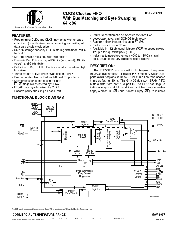
FUNCTIONAL BLOCK DIAGRAM
CLKA W/RA ENA MBA
Port-A Control Logic Parity Gen/Check
Bus Matching and Output Byte Swapping Register
MBF1 PEFB
ODD/
Mail 1 Register
Parity Generation
EVEN
Input Register
64 x 36 SRAM
Output Register
Device Control
64 x 36
Write...